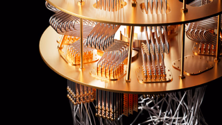
A fingernail-sized glass chip just set a record: 42.7 Gbit/s of quantum-certified random number generation[ScienceDaily]. That’s a measured result from researchers at the University of Padua, Politecnico di Milano, and Italy’s CNR Institute for Photonics and Nanotechnologies. The timing matters. Quantum computing threats to RSA and AES are no longer abstract conference fodder. NIST finalized its first post-quantum cryptography standards in 2024, and governments are racing to deploy quantum-safe infrastructure before harvest-now-decrypt-later attacks render today’s encrypted traffic worthless. A hardware source of physics-guaranteed randomness running at data-center line rates isn’t optional anymore. It’s the missing piece in a defense stack that needs to ship now.
The Breakthrough at a Glance
The core result is straightforward: a photonic chip, fabricated in glass waveguides, generates certified quantum random bits at 42.7 Gbit/s [ScienceDaily].
 Photo by
 Previous QRNG (quantum random number generator) devices in comparable form factors typically topped out in the low single-digit Gbit/s range. This chip clears that bar by roughly an order of magnitude.
The specs that matter for anyone evaluating deployment:
-
Throughput: 42.7 Gbit/s secure random bit generation
-
Insertion loss: approximately 1 dB, remarkably low for an integrated photonic device [ScienceDaily]
-
Common-mode rejection ratio: above 73 dB, meaning noise isolation is excellent
-
QKD capability: 3.2 Mbit/s secret key rate over a simulated 9.3-km fiber link
-
Stability: signal holds steady for hours with seamless fiber-optic connectivity
Glass as a substrate is the unsung hero here. Compared to silicon photonics or polymer waveguides, glass offers lower optical loss and better thermal stability. That translates directly to fewer calibration headaches in production environments.
How It Actually Works
The chip exploits quantum vacuum fluctuations, the irreducible noise floor of the electromagnetic field that exists even in a perfect vacuum.
 Photo by
 Laser light is split and recombined inside glass waveguides using integrated beam splitters and phase shifters. The quantum vacuum introduces tiny, physically unpredictable phase differences in the recombined signal. A homodyne detection scheme measures those differences at high speed.
Most QRNG vendors pitch “quantum randomness.” In practice, many commercial devices still lean heavily on post-processing to clean up classical noise they can’t fully separate from the quantum signal. This chip’s 73 dB common-mode rejection ratio suppresses classical noise aggressively enough that the raw quantum signal dominates before extraction algorithms even touch it. That’s what sets it apart.
Real-time randomness extraction runs at line rate, so there’s no buffering bottleneck between the photonic front-end and the digital output. The output continuously passes NIST statistical certification standards. Full photonic integration, with beam splitters, phase shifters, and detectors all on one chip, eliminates the bulky optical bench setups that made earlier QRNG systems impractical outside a lab.
Why 42.7 Gbit/s Changes the Game
Speed has been the quiet bottleneck in quantum-safe encryption.
 Photo by
 Modern data centers run 100G and 400G links. If your entropy source only produces 2 to 3 Gbit/s, you’re either rate-limiting your encryption pipeline or falling back to PRNGs (pseudo-random number generators) to fill the gap. That defeats the purpose.
At 42.7 Gbit/s, a single chip can seed encryption for several simultaneous 10G encrypted channels without becoming the throughput ceiling. That’s the difference between a lab demo and something a network engineer would actually deploy.
“The chip achieved a secure random bit generation rate of 42.7 Gbit/s, setting a record for this type of system.” [Forgedouble]
PRNGs are algorithmically deterministic. The 2012 Debian OpenSSL vulnerability, where weak PRNG seeding exposed thousands of SSH keys, showed what happens when “random enough” turns out not to be. Physics-based randomness eliminates that entire attack surface. At this throughput, the cost-per-random-bit drops sharply compared to software alternatives, making the economics viable for infrastructure-scale deployment rather than niche high-security enclaves.
Where It Deploys Today
Three sectors can integrate this chip without waiting for next-generation hardware.
 Photo by
 Financial infrastructure. High-frequency trading platforms execute millions of encrypted transactions per second, each requiring fresh cryptographic seeds. A QRNG chip at 42.7 Gbit/s can feed session key generation at transaction speed without becoming a bottleneck.
Hyperscale cloud. Cloud providers can embed the chip into existing HSMs (hardware security modules) to upgrade entropy generation with zero software changes. HSM vendors are already evaluating photonic QRNG integration for next-generation key management appliances.
Quantum key distribution networks. QKD deployments in China and Europe have consistently cited QRNG rate as a primary constraint on secure key refresh intervals. This chip removes that constraint. The demonstrated 3.2 Mbit/s secret key rate over a simulated 9.3-km fiber link confirms compatibility with existing QKD infrastructure .
Limitations Worth Knowing
Glass photonic chip fabrication requires specialized lithography that only a handful of foundries worldwide currently support.
 Photo by
 This isn’t something TSMC or Samsung can slot into existing process nodes tomorrow. Unit costs remain elevated. Estimates put photonic QRNG chips at 10 to 50 times the cost of equivalent PRNG software licensing, which means the value proposition is clearest for high-security, high-throughput use cases first.
Environmental sensitivity is another factor. Temperature swings and vibration can affect photonic component alignment. Data center deployments are fine since the environment is controlled. Edge and mobile deployments will need hermetically sealed, thermally stabilized packaging, adding both size and cost.
Neither of these is a showstopper, but they define the adoption curve: data centers and financial institutions first, consumer devices later.
What Comes Next
The research roadmap points toward three milestones:
 Photo by
 - Terabit-class throughput. Wavelength-division multiplexing across quantum channels on a single chip could push output beyond 100 Gbit/s. Four-channel prototypes are already in lab testing.
- CMOS integration. Intel and IMEC have published roadmaps for silicon photonic integration with CMOS logic nodes by the late 2020s. When quantum entropy generation lives on the same die as your processor, QRNG becomes invisible infrastructure rather than a bolt-on.
- Certification standards. NIST and ISO are developing hardware QRNG certification frameworks. Once those ship, enterprise and government procurement cycles will accelerate.
The gap between “works in a lab” and “ships in a product” is real, but this chip sits closer to the shipping side than most quantum hardware announcements. Insertion loss is low, fiber compatibility is proven, and the form factor fits existing rack-mount architectures.
A glass photonic chip generating 42.7 Gbit/s of quantum-certified randomness is a genuine inflection point, not because the physics is new, but because the engineering finally matches real-world network speeds. For teams managing encryption infrastructure at scale, the practical question has shifted from “when will quantum randomness be fast enough?” to “which integration path gets it into our HSMs first?” Reviewing NIST’s QRNG certification timeline and auditing current entropy sources against post-quantum threat models is a reasonable place to start. In a world where algorithmic randomness has been cracked before, physics-guaranteed randomness is becoming the new baseline.